Cx4 finished
The Cx4 FPGA core is complete. Check it out:
The Cx4 FPGA core is complete. Check it out:
I added a status page to reflect the current status, feature set, and progress of the project.

Cx4 memory map and data RAM are implemented. No work done on the actual core yet. Still, sometimes it’s nice to get any positive feedback from the hardware. 🙂
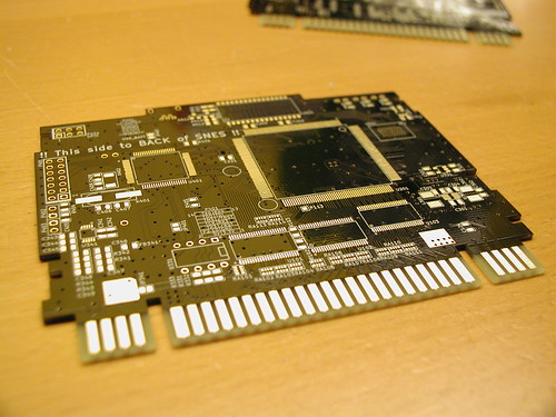
I had the Rev.E proto assembled by the end of August – but never got around to showing it off. 😉
Well, here it is.
The fat 4MBit SRAM at the top isn’t used yet. Its purpose is to retain save data in case of power failure (before it’s written to SD card), to serve as custom chip work RAM, and probably to store some other status information. Save data is currently stored in PSRAM along with the ROM, and monitored/saved to card from there.

Though the Zeroplus Logic Cube is rather low-end, it’s still a 200MHz, 128kSamples LA that has proven invaluable for all sorts of debugging. The JTAG/UART adapter (not shown) is a run-of-the-mill FT2232 DIP adapter board which plays nicely with OpenOCD. This one I got cheap from Akihabara (thanks to Tobias Diedrich!).

Quick update, the latest prototype PCBs arrived a couple of days ago. Assembly is in progress. This revision reduces audio noise from the DAC. This was a problem with 1CHIP SNESes which introduce much more noise, presumably due to their much steeper signal edges on the bus. The noise disappears when using a “custom chip game” case with the additional grounding prongs. I didn’t want to rely on that though, hence the hardware update. 😉
Here they are. I hope this is the last hardware revision, all those prototype PCBs are getting expensive…

I did this a while ago and thought it might be interesting. The 1CHIP SNES (1995~), with S-CPU, S-PPU1 and S-PPU2 united in a single chip (S-CPUN), has vastly improved picture quality over the old versions. Most notably the rising edges of the output signal are much steeper, resulting in sharper dark->bright transitions.
This is not an issue of the video encoder, it looks exactly the same via RGB (save for color balance).
Here are some examples to show the difference.
Sorry the pictures turned out quite big but it’s important not to lose any detail here. 😉
The images below show three frame captures from a “regular” SNES. Roll over them to see the 1CHIP version.


So the hardware was pretty much done at that point. Yet I did a complete redesign of the hardware. Why? Multiple reasons:

So that was a pretty big overhaul. The current result looks like this:

Development is now going on to implement the enhancement chips. The following are currently supported:
Development of sd2snes began in April 2009, inspired by sd2iec (hence the name).
Since 2001 I had been tinkering around with modified SNES cartridges, removing the ROMs to replace them with small self-made flash modules (usually a 29F032 or 29LV640 soldered on a small PCB with a pin header). They looked like this:

Even back then the idea to make a complete flash based cartridge from scratch was lingering in the back of my head. But it seemed too difficult to do for me. It also seemed impossible to implement new features, like additional memory maps, custom chips, etc. afterwards with the flexibility I wanted.
Fast forward to 2009. With time, more powerful yet affordable FPGAs had become readily available. Also sd2iec was released which provided ready-made SD card support (SPI mode).
The first prototype was constructed on breadboard with lots of self made adapters, most notably the FPGA->breadboard adapter, with on board power supply and configuration jumpers.

Hardware specs of the breadboard were:
This design was more or less adapted for the first PCB prototypes (all of Mk.I), the only difference being more SRAM (64MBits). Loading was somewhat slow due to SPI mode and a maximum 6MHz SPI clock from the AVR. Later the FPGA was used to load blocks to RAM directly, increasing the read speed to ~1.5MB/s. SNES master clock (Pin 1) was used as a clock source for the FPGA. It proved unreliable (the DCM just stopped working at random) so in later revisions (and all of Mk.II) the AVR clock output was used to clock the FPGA. This resulted in the last revision of Mk.I having the additional groups of slot pins removed entirely.


Coming up: SuperCIC, MSU1, timing perils