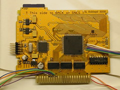
A small recap, part 2
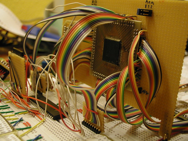
So the hardware was pretty much done at that point. Yet I did a complete redesign of the hardware. Why? Multiple reasons:
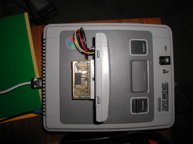
- Segher reverse engineered the SNES CIC and published the disassembled ROM dump of the D411 (US/JP CIC). I figured out the seeds of the D413 (EU CIC) – just one nibble was changed – and made a PIC based CIC replacement with automatic region fallback. sd2snes now worked on any unmodified SNES. (Also a counterpart was created later to replace the original CIC in the console itself – with additional features like switchless 50/60Hz switching. See the SuperCIC page.)
- MSU1 – byuu came up with the 21fx specification, later renamed to MSU1, that allows streaming of up to 4GB of data and CD-quality audio playback from mass storage. The present hardware would not have been able to stream data from card at the rate required by the spec. Also a DAC was needed to input audio to the SNES’s cartridge slot. Additionally the bonus extension pins of the cartridge had to be added again to accomplish this – to access the line-in and to synchronise audio with the SNES master clock to maintain A/V sync during video playback.
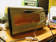
- RAM cost and space requirement. The 64 MBits of SRAM were comprised of four 16 Mbit SRAM chips at ~14€ each. A 128Mbit PSRAM is now used. There was a catch though – these chips are only available in BGA packages. A subproject was initiated to modify a pizza oven to work as a makeshift reflow oven. I was skeptical at first but it proved to work better than expected.
- A second RAM bus was added. This was necessary to allow for parallel access to the ROM and battery/cartridge RAM areas. Some custom chips like the SuperFX require this. The second RAM is 4Mbits of SRAM. The increased number of required I/Os required changing the FPGA to a bigger package (PQ208).
- Due to MSU1 the loading speed had to be improved. A more advanced microcontroller (ARM Cortex M3 @100MHz) was used to replace the slow 8-bit AVR. This chip also includes an RTC so a battery holder was added to maintain the RTC. The battery doubles as a backup battery for the 4Mbits of SRAM. That way saved games can be preserved even when a blackout occurs before the automatic save feature can write to SD card.
- I replaced Eagle with KiCAD as the EDA tool – it is free as in speech, less restricted, and slightly more usable.
- Much higher loading speed (9MB/s)
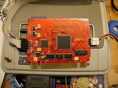
So that was a pretty big overhaul. The current result looks like this:
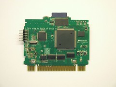
Development is now going on to implement the enhancement chips. The following are currently supported:
- S-RTC
- BS-X / Satellaview
- DSP1
- DSP1b
- DSP2
- DSP3
- DSP4
- ST0010
- MSU1
