Status update – important stability fixes
Oof! Well, looks like I couldn’t help but take a deep dive down the rabbit hole after all, staring at scope and LA traces for weeks to find the root causes for some random glitches and freezes. And successfully at that.
Exhibit 1: The Open Bus Glitch
Hiding in the dark places between CPU cycles this should have no effect on normal operation (except when relying on certain open bus behaviour). What it does is put a value on the bus just inbetween two cycles so no one should ever notice… only to strike when you least expect it!
This bug was first brought up in a different form by the TASBot community and I’ve gotten some tremendously helpful details and troubleshooting from them. Those people really push the technical boundaries to make miracles happen.
Here’s the lowdown: Should you decide to innocently write to PPU register $2100 to change the brightness mid-screen, something nasty might happen. PPUs latch the written value on EVERY 21MHz tick as long as the write cycle is ongoing, not just at the end of it. So it will ALWAYS latch invalid data appearing at the beginning of a cycle, before it can turn valid. In case of forced blanking, this will turn off sprite fetching for just a bit but enough to cause image corruption.
This is an SNES bug at the core – and one you might only ever notice while trying to work around another serious SNES DMA bug like Near did – HDMA to $2100 can break the DMA engine on S-CPU A – but that’s a story for another day.
Just do something mundane like “lda.b #$0f : sta.l $802100” somewhere mid-screen during HBlank and see what happens. The “$80” from the last byte of the second instruction will carry over to the beginning of the PPU write, briefly turning on forced blanking until the CPU asserts the value “$0f” on the bus.
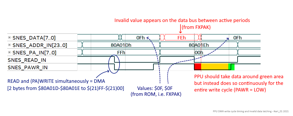
The sd2snes/FXPAK just has the “ability” to make this glitch appear even though your data would not normally have the forced blanking bit set at all, by sometimes leaking RAM data on the bus that is not intended for it. This happens because it uses the CPU clock signal’s falling edge to determine that the SNES cycle is over and starts using the RAM for other things like save state or SRAM monitoring. However, since the READ signal is still active it will still output whatever comes from RAM to the SNES bus!
It is a specialty of SNES DMA access timing that the A-Bus READ pulse is substantially longer than the CPU clock active pulse; therefore data from any subsequent use of the RAM can be put on the bus as long as the SNES READ signal is still active.
Sometimes the data output is then turned off during data line toggles, resulting in funny in-between levels like this one:
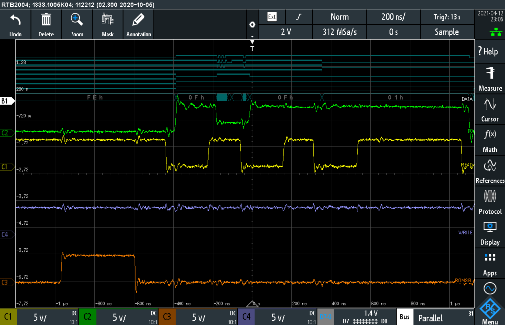
This is something you wouldn’t catch using just a logic analyzer.
The issue was eventually fixed by generating a combined “SNES_PULSE” signal that will stay active until the end of whatever is the longest active pulse so RAM is never cut off as long as the data bus output is active.
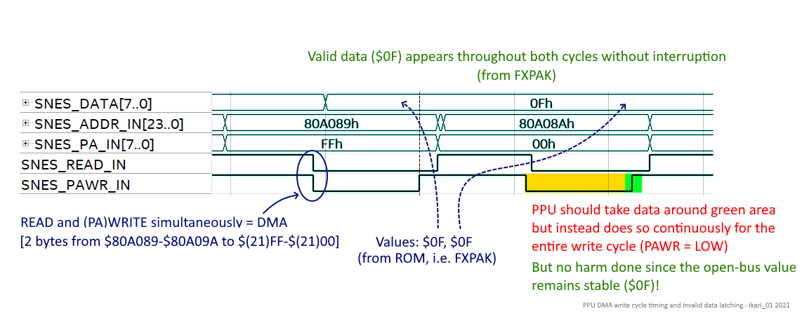
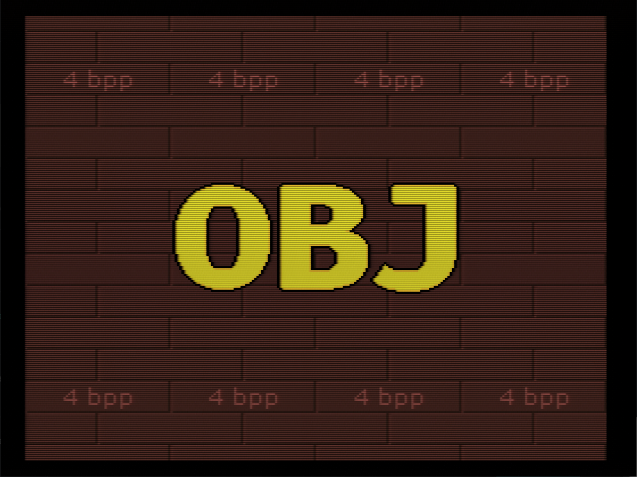
Exhibit 2: The Coupling Chain Reaction
Causing all sorts of crashes and glitches, but sort of unpredictable and sporadic; e.g. graphical glitches in various games, such as Super Mario RPG or Another World, or random crashes.
It rarely happens but during testing and fixing the timing for the Open Bus Glitch I happened to unmask the effect so it happened much more often – which is a good thing because I was finally able to pinpoint it.
The cause is not unlike the Open Bus Glitch but it happens at the beginning of the cycle, not at the end, and its effect is different.
At the beginning of a read cycle the address has typically been valid long enough for the RAM data to have settled. But sometimes the data is not valid yet because the RAM read might be postponed a bit because an FXPAK-internal access is served (as above, e.g. for SRAM monitoring). In this case the previous value from RAM is put on the bus briefly before the correct one appears. In some cases this causes rapid toggling of all eight data bus lines, depending on the data constellations used by the game.
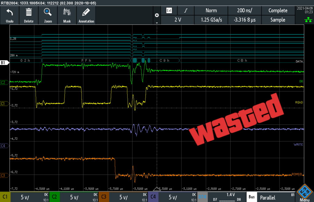
The rising edges couple into all other lines and momentarily make a wrong address appear on the bus – this in turn causes the FXPAK to fetch an incorrect data byte in the middle of the read cycle. The resulting change in data lines can glitch the other signals again, etc… what the SNES CPU sees is often a mixture of bits from multiple addresses; it then reads a wrong instruction or data, execution flow gets disrupted sooner or later.
In the picture above, Another World / Out Of This World is running and executing at $80E513-$80E514:

You can see the last byte of the “lda $0260, x” instruction to the far left of the oscilloscope trace (“02”, near the “B1>” label). The SNES CPU then executes the actual instruction, fetching two bytes from SNES WRAM ($800260) which happen to be the value $FFFF.
Things go awry on fetching the following instruction byte: after READ (yellow trace) goes low, all data lines (the 8 teal colored traces at the top) momentarily go down at once, then quickly up again. The coupling becomes easily visible in the other traces (READ, WRITE, and ROMSEL which is part of address decoding on the SNES); all of them show a significant spike before returning to normal. The FXPAK also sees these spikes and acts upon them accordingly, putting incorrect values on the DATA bus.
The CPU reads the mixture of data bits as $DB instead of $C9 – turning the harmless CMP instruction into an STP instruction which halts the CPU immediately! There is no more activity after that fetch, and the data bus is left floating – you can see the open bus voltage gradually decreasing toward the right end (D0, green trace). The game has crashed and the CPU is essentially dead until a system reset is performed.
For now this issue is fixed by enabling the data bus only when it is safe to assume that the RAM value has settled and any data line toggling is masked from the SNES data bus.
There is room for improvement here. Currently the RAM-to-SNES data path, including address mapping, bus enable and direction switching, is end-to-end combinatorial. An ideal fix for both of these issues would be a partial rewrite of the memory sharing mechanism so it actually buffers RAM data for the SNES bus. This would separate RAM access timing from the actual SNES bus timing with the added benefit of having more free time for shared RAM access.
Progress on current firmware release
Both of the issues mentioned above have been fixed for the base FPGA configuration only so far.
I made improvements to the save state fix data format so it can support more flexible fixes; this was required to make Star Ocean (uncompressed) work with save states.
VRAM DMA mirroring didn’t work properly depending on the source of the data – it didn’t take SRAM into account as a cartridge-based source and tried to sniff the values off the SNES data bus. This led to corrupted party stats in Near’s Bahamut Lagoon translation when loading a save state and has been fixed.
Saving / loading states has been refined a bit for MSU1 so it mutes the audio while accessing the SD card and doesn’t produce a buzzing sound.
I fixed the YAML parser so it can handle multi-line lists with comments in the first line which is good for clarity in the savestate fixes YAML file for games that need multiple fixes.
Next steps:
- The fixed bus timings now need to be ported to all the other cores (DSP, SuperFX, SA-1, etc.) which should take 2-3 hours of work (and 3-4 days of Xilinx compile time. 😅)
- Perform some testing on USB features to make sure everything is basically working
- Check why cheats might not be working (has been reported as an issue)
- Release a beta 😉